This product replaced byIPC 7525B - Stencil Design Guidelines This product replacesIPC 7525 - Stencil Design Guidelines Browse Product Family. IPC-7525 Stencil Design Guidelines ASSOCIATION CONNECTING ELECTRONICS INDUSTRIES 2215 Sanders Road Northbrook IL 60062-6135 Tel.

Ipc 7525 Stencil Design Guidelines
Stencil Design Guidelines Most Recent.
. During the initial Stage of Stencil design it is imperative to arrest these problems. Michael Roesch and J Franke Stencil Design Guidelines for Robust Printing Processes in Electronics Production Considering Stencil and Solder Paste. This includes differences for tin lead and lead free solder paste overprint two-print and step stencil designs.
It is intended as a guideline only. Laser-cut with electropolish for better release than the regular laser-cut stencil. DESIGN AND ASSEMBLY PROCESS IMPLEMENTATION FOR BOTTOM TERMINATION COMPONENTS.
STENCIL AND MISPRINTED BOARD CLEANING HANDBOOK. It is intended as a guideline only. 14 Problem Statement Proper stencil cleaning should remove all solder particles and flux vehicle organics from stencil apertures without damaging the stencil bonding adhesives and elastomer frame.
The paper presents the innovative technology of step-up and step-down stencils in a laser cutting and laser welding process. 830 am - 6 pm EST. According to IPC design guidelines 7525B there should be 89mm 035 keep-out between the step down and the aperture in the step down area for every 025mm 001 of step height.
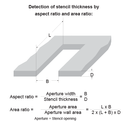
Appendix A provides definitions for terms used in this handbook. Stencil Design Guidelines 1 PURPOSE This document provides guides for the design and fabrica-tion of stencils for solder paste and surface-mount adhe-. This standard establishes the guidelines for the design and fabrication of stencils for solder paste and surface mount adhesive with discussion on through-hole mixed technology and includes the differences for tin lead and lead-free solder paste overprint two-print and step stencil designs.
Thinner stencil foil but print other devices using a thicker stencil foil. Package pitches 065mm can accommodate a 6-mil thick stencil. Standard by Association Connecting Electronics Industries.
IPC 7525A Stencil Design Guidelines. IPC-7525A Stencil Design Guidelines Developed by the Stencil Design Task Group 5-21e of the Assembly and Joining Processes Committee 5-20 of IPC Users of this publication are encouraged to participate in the development of future revisions. February 2007 Stencil Design Guidelines.
It is intended as a guideline only. Stencil Design Guidelines 1 PURPOSE This document provides a guide for the design and fabrication of stencils for solder paste and surface-mount adhesive. IPC 7525B IPC.
Design of Stencil should comply with IPC-7525A. A sample order form and user inspection checklist are also included. Chip component aperture design.
IPC-7525A -标准资料文件pdfIPC-7525A Stencil Design Guidelines Working Draft 1 February 2004 ASSOCIATION CONNECTING ELECTRONICS INDUSTRIES 2215 Sanders Road Northbrook IL 60062-6135 Tel. The FileOpen Plug-In works with Adobe Reader and other viewers. STM STENCIL DESIGN AND CONSIDERATION BASE ON IPC Page 6 of 34 02062007 of circuit design into an organized manner that will give the same function as physical wiring.
Stencils are usually made of stainless steel. This document provides guidelines for the design and fabrication of stencils for solder paste and surface mount adhesive with discussion on through-hole and mixed technology. Documents sold on the ANSI Webstore are in electronic Adobe Acrobat PDF format however some ISO and IEC standards are available from Amazon in hard copy format.
K2 is the distance between the step-down wall and an aperture in the thicker part of the stencil. Ad Find them all on the ANSI Webstore. Definitions denoted with an asterisk below are reprints from IPC.
Stencil Design Guidelines 1 PURPOSE This document provides guides for the design and fabrica-tion of stencils for solder paste and surface-mount adhe-sive. Ences that may need to be considered in the stencil clean-ing process. IPC-7525 Revision C November 2021 - Stencil Design Guidelines.
The step-upstep-down stencil is a special development for the adjustment of solder paste quantity fulfilling the needs of placement and soldering. May 2000 Stencil Design Guidelines. Much of the content is based on the experience of stencil designers fabricators and users.
In order to read a Secure PDF you will need to install the FileOpen Plug-In on your computer. The recommended design for K2 keep-out is a minimum of 25 mils 065 mm. Contribution is from screen-printing process where stencil design plays major role if considered other screen-printing parameters are optimized on which this paper is focused on.
11 Terms and Definitions All terms and definitions used throughout this handbook are in compliance with IPC-T-50. October 2011 Stencil Design Guidelines Historical Version. TERMS AND DEFINITIONS FOR INTERCONNECTING AND PACKAGING ELECTRONIC CIRCUITS.
Standards Referencing This Book- Show below - Hide below IPC T 50. 8475099700 Fax 8475099798 IPC-7525A st 1 Working Draft February 2004 1 PURPOSE This. IPC 7525 suggests K1 should be a minimum of 35 mils 09 mm for every 1 mil 0025 mm of step-down thickness.
4- or 5-mil thick stencil is recommended for 050mm pitch packages. IPC-7525A - February 2007 IPC-7525 - May 2000. IPC 3000 Lakeside Drive Suite 309S Bannockburn Illinois 60015-1249 Tel 847 6157100 Fax.
Print from PDF Association Connecting Electronics Industries Standards. Design of Stencil should comply with IPC-7525A. This document provides guidance for the design and fabrication of stencils for solder paste and surface-mount adhesive.
During the initial Stage of Stencil design it is imperative to arrest these problems. Secure PDF files include digital rights management DRM software. This includes differences for tin lead and lead-free solder paste overprint two-print and step stencil designs.
The IPC stencil guidelines are the most commonly used and are a good starting point however they do not take into account outside variables that regularly come up in all manufacturing lines such as environmental conditions oven profile printing variables squeegee pressure under-board support squeegee speed etc. A sample order form and user inspection. DRM is included at the request of the publisher as it helps them protect their copyright by restricting file sharing.
IPC75252000-Stencil Design Guidelines-Customer Service. The relationship of SMT component PCB lay-out and PCBA process are discussed in two steps. Tolerances must be tightly.
Much of the content is based on the experience of stencil designers fabricators and users. Contribution is from screen-printing process where stencil design plays major role if considered other screen-printing parameters are optimized on which this paper is focused on.
2

Csn33 Micron Bga Manufacturer S User Guide

Ipc 7525c

Ipc 7525 A Stencil Design Guidelines Pdf Docer Com Ar
Smd Stencils Design Aid Multi Circuit Boards
Ipc 7525a 2007 Stencil Design Guidelines
Ipc 7525c

Ipc Document Revision Table Ipc International Inc
0 komentar
Posting Komentar